Researchers Realize the Direct Uniform Graphene Monolayers Growth on Dielectric Substrate by Metal-Free Chemical Vapor Deposition
Direct chemical vapor deposition (CVD) growth of high-quality graphene on dielectric substrates holds great promise for practical applications in electronics and optoelectronics without any complicated transfer process. However, graphene growth on dielectrics always suffers from the issues of inhomogeneity and/or poor-quality owing to the absence of metal catalysts.
Previous works mainly developed the metal-assisted or plasma-enhanced growth to solve the drawback of poor innate catalytic activity of dielectrics in the realm of direct graphene growth on dielectric substrates. However, graphene grown on dielectric substrates usually featured with slow growth rate and multiple nucleation, thus likely evolving graphene films with uncertain thickness and non-uniformity.
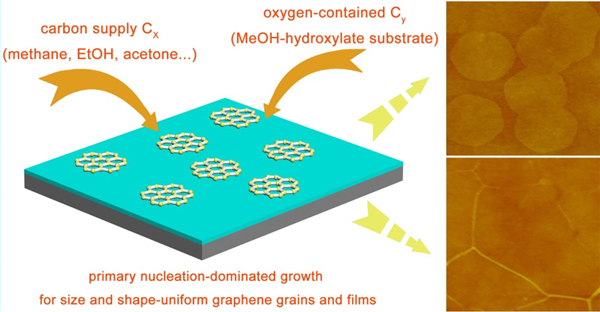
To realize the direct uniform graphene monolayers growth on dielectric substrate, researchers utilized a novel precursor-modification strategy by mixing methanol with other precursors with higher carbon content. The decomposition of methanol would produce very trace amount of water with the aid of O2 released from SiO2 substrate, which moderately hydroxylated the substrate. Theoretical calculations indicated that the hydroxylation of SiO2 substrate can avoid the strong binding between graphene edge and silicon atoms on the SiO2 surface, thus facilitating the graphene edge growth and suppressing the secondary nucleation of graphene.
Benefiting from the primary nucleation-dominated mechanism, graphene grains and monolayer films with uniform shape and size were directly grown on dielectric substrates. Field effect transistor(FET) device characterizations of the as-grown uniform monolayer graphene indicate its outstanding electrical performance with carrier mobility up to 3800 cm2 V-1 s-1. Without any complicated transfer process, this controllable and facile method to prepare high-quality graphene film on dielectrics makes a step forward for high-performance graphene applications in integrated electronics and optoelectronics.
The research team includes a group led by Prof. YU Gui from Institute of Chemistry, Chinese Academy of Sciences, and a group led by Prof. XU Zhiping from Applied Mechanics Laboratory, Department of Engineering Mechanics and Center for Nano and Micro Mechanics, Tsinghua University. The research was supported by “National Natural Science Foundation of China” and “the Strategic Priority Research Program of the Chinese Academy of Sciences”.

Primary nucleation-dominated chemical vapor deposition growth for size and shape-uniform graphene grains and films. (Image by Prof. YU Gui)
The work was published in J. Am. Chem. Soc., 2019, 141, 11004?11008. (Primary Nucleation-Dominated Chemical Vapor Deposition Growth for Uniform Graphene Monolayers on Dielectric Substrate)
Contact:
Prof. YU Gui
Institute of Chemistry, Chinese Academy of Sciences
E-mail: yugui@iccas.ac.cn


