Beaded Cobalt Oxide Nanoparticles along Carbon Nanotubes: Towards More Highly Integrated Electronic Devices
Lei Fu Zhimin Liu Yunqi Liu* Buxing Han Pingan Hu Lingchao Cao and Daoben Zhu*
The miniaturization of components for the construction of electronic and optical devices is an essential feature of modern technology. It is becoming apparent that current “top-down” lithography-based techniques are growing increasingly complicated with attempts to achieve further miniaturization. Consequently “bottom-up” routes toward nanometer-scale electronics including the use of nanoparticles (NPs) carbon nanotubes (CNTs) or nanometer-scale metallic or semiconductor wires as functional building blocks for electronic devices are required. However unduly separate blocks depress the degree of integration which runs counter to the mainstream of modern electronics. The ability to organize and interconnect NPs using inorganic nanotubes or nanowires is an important step toward fabricating highly densely integrated nanometer-scale functional devices. Unfortunately only few reports provide simple efficient routes for wiring NPs using nanotubes or nanowires.
We report how multiwalled carbon nanotubes (MWCNTs) beaded with spherical crystalline Co3O4 NPs have been successfully synthesized based on a simple low temperature supercritical-solution method. These particles have the same diameter and are distributed along the axis of a carbon nanotube like a necklace (Figure a b). Although our initial efforts have focused on Co3O4 and MWCNTs the synthesis method can be readily extended to other transition metal oxides and one-dimensional nanomaterials by the introduction of the appropriate precursors into the reaction chamber. The beaded one-dimensional nanomaterials provide an opportunity for fabricating highly densely integrated nanometer-scale functional devices. We have also fabricated a Schottky-junction diode utilizing individual “beaded” nanotubes and studied its electrical transport properties (Figure c). The measured current-voltage characteristic exhibited clear rectifying behavior and no reverse bias breakdown was observed up to a measured voltage of 2.5 V.
Advanced Materials 2005 Vol.17 No.2 p217-221
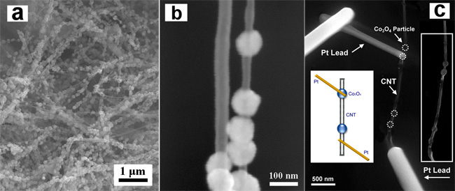
Figure a. Low-magnification SEM image of the product showing a large quantity of necklace-like nanostructures.
Figure b. Enlarged image of the representative morphology.
Figure c. SEM image of an example of MWCNT/Co3O4 NP with Pt contacts.