N-type organic semiconductors are important components in light-emitting diodes field-effect transistors and solar cells. Compared to p-type organic semiconductors good n-type organic semiconductors especially polymers remain rare.
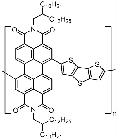
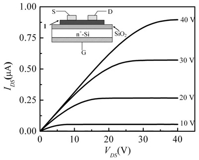
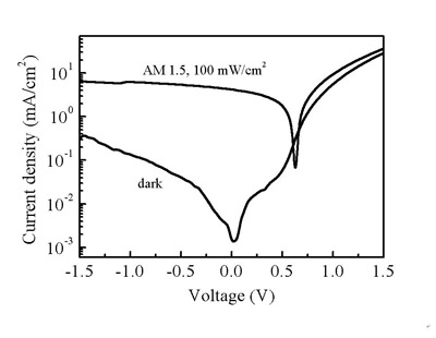
Under the financial supports of National Nature Science Foundation of China Ministry of Science and Technology of China and Chinese Academy of Sciences researchers at Institute of Chemistry Chinese Academy of Sciences collaborated with researchers at Georgia Institute of Technology USA synthesized a new solution-processible conjugated polymer (1 Figure 1) based on alternating dithienothiophene and perylene diimide (PDI) units. The polymer exhibits high electron mobility excellent thermal stability high electron affinity and appears almost black due to strong absorption throughout the visible and extending into the near-IR. With the polymer as n-type material the researchers fabricated high-performance organic field-effect transistor (OFET) and all-polymer solar cell (PSC). An electron mobility of 1.3 ´ 10-2 cm2V–1s–1 a low threshold voltage of ca. 4.4 V and an on/off current ratio of >104 were obtained from the OFETs based on 1. The electron mobility of 1 is among the highest obtained for the solution-processed OFET based on n-type conjugated polymers. The all-polymer PSC based on a blend of 1 (acceptor)/bi(thienylenevinylene)-substituted polythiophene (donor) exhibits an average power conversion efficiency over 1% under the illumination of AM 1.5 100 mW/cm2 which is among the highest achieved to date in the all-polymer PSCs.
J. Am. Chem. Soc.(2007 Vol. 129(23), 7246-7247)

Figure 1. Chemical structure of polymer 1

Figure 2. Current-voltage characteristics (IDS vs. VDS) at several values of the gate voltage (VGS) for a top contact device with W = 2000 m L = 200 m and 100 nm of 1.

Figure 3. Current density-voltage characteristics of a device with the structure ITO/PEDOT:PSS/1:2 (1:1 w/w)/Al in the dark and under the illumination of an AM 1.5 solar simulator 100 mW/cm2. , |
