ICCAS realized optical signal manipulation based on the coupling effect of excitons and surface plasmons
In comparison with electronic devices, optical devices have advantages of high speed, broad bandwidth, and low driving power, which are crucial for the realization of nanophotonic circuits for next-generation all optical information processing.
In recent years, Prof. YAO Jiannian and ZHAO Yongsheng’s groups in the Key Laboratory of Photochemistry in the Institute of Chemistry, the Chinese Academy of Sciences (ICCAS) have studied the design and fabrication of photonic devices based on the low-dimensional organic nanomaterials (Acc. Chem. Res.,2010,43,409-418, Adv. Funct. Mater., 2012, 22, 1330-1332). They have developed various nanophotonic devices such as nanolasers (J. Am. Chem. Soc., 2011, 133, 7276-7279), sub-wavelength optical waveguide (Adv. Mater., 2011, 23, 1380-1384), photonic routers (J. Am. Chem. Soc., 2012, 134,2880-2883) and photodector (Adv. Mater., 2012,24, 2332-2336). These works demonstrated the great potential of the low-dimensional organic materials in the field of nanophotonics and paved the way for the fabrication of complex functional photonic devices.
Most of the present optical devices have lateral dimensions on the order of micrometer due to the diffraction limit, which makes it difficult to integrate these components with the electric circuits on nanometer scale (about 50 nm). Therefore, it is of great significance to scale down the size of the photonic devices. In recent years, metal nanowires with diameters of tens or hundreds nanometer have attracted increasing attention due to their ability to guide light below the diffraction limit in the form of surface plasmon polaritons (SPPs). SPPs are special electromagnetic fields with unique physical properties in polarization, mode volume and dispersion characteristic which make them promise for the realization of plasmonic devices. However, the ohmic loss inhibits the transfer of optical signals across an entire circuit (about 1mm) solely with plasmonic waveguide. Therefore, a simple and convenient strategy is required to integrate plasmonic modules with low-loss dielectric waveguides for information processing.
Recently, under the supports of the National Nature Science Foundation of China, the Chinese Ministry of Science and Technology, the Chinese Academy of Sciences, and Institute of Chemistry, they successfully prepared organic/metal nanowire heterojunctions with the site-specific growth of gas phase organic molecules. The strong coupling between exciton polaritons (EPs) and SPPs at the organic/metal interfaces could substantially enhance the launch efficiency for SPPs. Furthermore, the intensity of the optical signals in silver nanowire exhibits a strong dependence on the polarization of the incident light. Based on this modulation method, optical logic operations under subwavelength scale were realized in individual heterojunctions. The results have been published in Adv. Mater., 2012,24, 5681–5686, and selected as the cover story (Figure 1).
In order to transfer the logic calculation results to the target output ports, they have further developed directional couplers to manipulate multiple optical signals. Branch-like organic/metal nanowire heterostructures were successfully fabricated by embedding multiple metal nanowire branches in organic microwire trunks during the self-assembly in liquid-phase. Based on the angular dependence of photon-plasmon coupling, light signals inputted from the organic waveguide could be selectively transported to the predetermined subwavelength metal branches. The excellent performances in directional signal transfer provide a new strategy to realize the optical multiplexers with multiple input/output ports. The results have been published in Adv. Mater., 2013, 25, 2784-2788, and selected as the back cover (Figure 2).
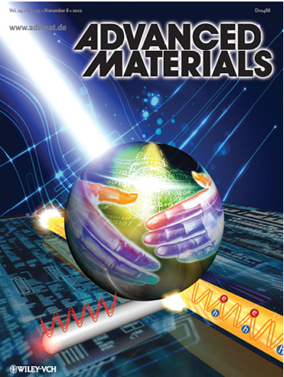
Figure 1 Cover story: The coupling between EPs and SPPs in organic/metal nanowire heterojunction(Image by ZHAO Yongsheng)
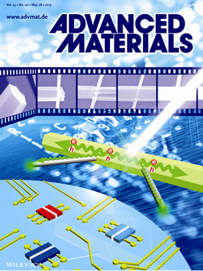
Figure 2 Back cover: The coupling between EPs and SPPs in organic/metal nanowire heterostructures and their application for the manipulation of multiple optical signals(Image by ZHAO Yongsheng)