Progress of Organic/Polymer Semiconducting Micro-/Nanocrystals
Single crystals could show intrinsic charge-transport properties and high mobility because of the perfect order of molecules, the absence of grain boundaries andthe minimized concentration of charge traps in single crystals, provides the opportunity for the revealing of the relationship between the microscopic molecular packing and macroscopic charge transport of the materials. Moreover, the study of organic single crystals is also crucial for the design of new organic semiconductors and the fabrication of high performance devices. Enormous recent efforts have brought significant progresses in the growth of organic single crystals, the fabrication of single crystal field-effect transistors (SCFETs), and the investigation of structure-properties relationship of organic semiconductors based on the crystals.
Organic field-effect transistors (OFETs) require semiconductors with high crystallinity so that few defects (e.g. disorders, grain boundaries) are contained in the semiconductor layer. Triarylamine derivativesare well known amorphous molecular glasses with low mobility (at around 10-4-10-5 cm2/Vs), which limits their application in OFETs. In this article, a cyclic triphenylamine dimer was demonstrated with high crystallinity. Micrometer and nanometer sized single crystalline ribbons could be produced easily by physical vapor transport technique. Field-effect transistors of the single crystalline ribbons exhibited mobility up to 0.05 cm2/Vs. To the best of our knowledge, it should be one of the highest mobility of triarylamine derivatives. Moreover, it was found that the mobility of the devices depended greatly on the size of the ribbons, the smaller the ribbons, the higher the mobility. It indicated “small” crystals were more proper for the fabrication of high performance devices (Adv. Mater. 2009, 21, 1605-1608).
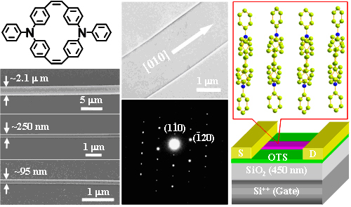
Figure 1 Micro- and nanometer sized single crystals of a cyclic triphenylamine dimer.
Organic crystals always exist as micro or nanometer sized crystals because of the weak intermolecular interactions of organic compounds, which presents a great challenge for the fabrication of devices, especially for the study of anisotropic transport property of such “small” crystals. Here, hexagonal micrometer sized organic single crystals of a fused-ring thienoacene, dibenzo[d,d′]thieno[3,2-b;4,5-b′]dithiophene (DBTDT), are synthesized controllably by physical vapor transport technique in large area. A “two-dimensional organic ribbon mask” technique is developed to fabricate organic field-effect transistors based on an individual microcrystal. The transistors exhibit mobility as high as 1.8 cm2V-1s-1 with on/off ratio typically >107. Multi-channel transistors along different crystal axes and crystal planes are fabricated to probe the transport anisotropy of the microcrystal. The mobility anisotropy along c and a axes is found at about 2-2.5, which coincides with the fact that the intermolecular interaction is the strongest along the c axis and the weakest along the a axis (Adv. Mater. 2009, 21, 1605-1608).

Figure 2 Anisotropic transport study of micro or nanometer sized crystals.
Micro- and nanometer-sized single crystalline disksof di(phenylvinyl) anthracene (DPV-Ant) were produced by physical vapor transport technique. Single crystalline transistors of the disks were fabricated by “organic ribbon mask” method. The mobility of the transistor based on the individual disk approached ~4.3 cm2V-1s-1. Mobility anisotropy along different crystalline axes of the disks was also studied. The anisotropy ratio was at around 1.5-1.95 (μa/μb), which coincided well with the fact that the stronger the intermolecular interaction is, the higher the mobility is. High performance inverters were fabricated with the integration of the p-type single crystalline transistors. The maximum gain of the inverters reached ~80 (Adv. Mater. 2009, 21, 3649-3653).

Figure 3 High performance organic single crystal transistors and digital inverters of an anthracene derivative.
Organic single crystal transistors and circuits are assembled by nanomechanial manipulation of nanowires of CuPc, F16CuPc and SnO2:Sb. The devices exhibit low operational voltage, high mobility and excellent air stability. The complementary circuits of the nanowires demonstrate versatile functions such as inverters, NOR, and NAND gates. The inverters exhibit sharp switching and high gain, and the logic circuits of NOR and NAND demonstrate ultra low power consumption (<40 pW). In combination with generic “bottom-up” assembly methods developed for nanowires this opens up for new opportunities based on tailor made organic building blocks (Adv. Mater. 2009, 21, 4234-4237).

Figure 4 Organic single crystal circuits.
Up to date, crystals of conjugated polymers have been rarely addressedregardless of their great advantagesin solution-process, large area device fabrications, mechanical flexibility and the incorporation of functionality by molecular design. Therefore, it remains challenging topics to obtain high-quality, single crystalline polymer nanowires for the study of intrinsic charge-transport properties of polymer semiconductors as well as the realization of high-performance polymer electronic devices. Here, we show that well-defined, highly crystalline nanowires of a rigid rod conjugated polymer, poly(para-phenylene ethynylene)s derivative with thioacetate end groups (TA-PPE) can be obtained by self-assembling from dilute solution. Structural analyses demonstrate the nanowires with an orthorhombic crystal unit cell wherein lattice parameters of a~13.63 Å, b~7.62 Å, and c~5.12 Å; and in the nanowires the backbones of TA-PPE chains are parallel to the nanowire long axis with their side chains standing on the substrate. The transport properties of the nanowires examined by organic field-effect transistors (OFETs) suggest the highest charge carrier mobility approaches 0.1 cm2/Vs with an average values at ~10-2 cm2/Vs, which is 3-4 orders higher than that of thin film transistors made by the same polymer, indicating the high performance of the one-dimensional polymer nanowire crystals. These results are particular intriguing and valuable for both examining the intrinsic properties of PPEs polymer semiconductors and advancing their potential applications in electronic devices(J. Am. Chem. Soc. 2009, 131, 17315-17320)。