Micro-scale organic waveguides and lasers based on 1D small-molecular nanostructures
Ever increasing attention has been paid to one-dimensional (1D) nanomaterials because the two-dimensional quantum confinement effect makes them promising as building blocks for the future miniaturized optoelectronic devices, such as waveguides, lasers, and so on. Most of the research works, however, have been focused on inorganic nanomaterials while little attention has been paid to organic ones, mainly because of the difficulty in the availability of 1D organic ones, especially those single-crystalline ones. In their recent works, Prof. Jiannian Yao and co-workers developed an adsorbent-assisted physical vapor deposition (PVD) method for the fabrication of crystalline organic nanowires with single composition in which the introduction of adsorbents was proven to be indispensable for improving the uniformity of the products (see Chem. Mater. 2006 18 2302-2306; Adv. Funct. Mater. 2006 16 1985-1991; Adv. Mater. 2007, 19, 3554-3558; Adv. Mater. 2008, 20, 79-83.)
Recently with supports of the National Natural Science Foundation and
Furthermore, they prepared two kinds of microstructures with rectangular and square cross-sections, respectively from a low-molecular-weight organic compound, BPEA, and extended the application of miniaturized sub-wavelength optical waveguide from solid wires and ribbons to hollow tubular structures. The single tube/rod characterizations indicate that the 1D BPEA microstructures can serve as active optical waveguides that allow the locally excited photoluminescence to propagate along the length of the 1D materials and out couple at the tube/rod tips. The tubular structures reveal lower optical loss during the light propagation compared with that of the solid rods. The optical loss in the microtubes is mainly from the re-absorption, while for the microrods, the predominant loss sources are scattering and the coupling between the rods and the substrates. The prepared 1D BPEA microstructures can serve as both single tube/rod and inter-tubes/rods active optical waveguides. (Angew. Chem. Int. Ed. 2008, 47, 7301–7305)。
Angew. Chem. Int. Ed. 2008, 47, 7301–7305
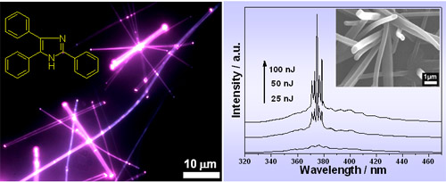
Left: PL microscopy image of TPI nanowires; Right: Power-dependent emission spectra of a TPI wire, inset, SEM image of TPI wires.